

Stepped Impedance Filter
- Robert Fennis
- Jul 24, 2025
- 3 min read

Updated: Aug 18, 2025
In this demonstration we will look at demo file 1 in the EMerge examples.
A stepped impedance filter is a low-pass filter realized in transmission line segments of varying impedance. Impedance values lower than line impedance look like capacitors to ground and high-impedance lines look like series inductors. We will not go into detail on the theory of these lines and instead stick to the implementation in EMerge.
We start with the basic required lines, importing EMerge and setting the basic constants.
The line length and width of the stepped impedance filter are contained in L0/W0 to L3/W3. The 3rd section is the middle section after which it simply reverses. L0 and W0 are the feed lines. We thus get:
L0, L1, L2, L3, L2, L1, L0
Same for the width
import emerge as em
import numpy as np
from emerge.plot import smith, plot_sp

mm = 0.001
mil = 0.0254*mm

L0, L1, L2, L3 = 400, 660, 660, 660
W0, W1, W2, W3 = 50, 128, 8, 224

th = 31
er = 2.2

Hair = 60

pcbmat = em.Material(er=2.2, tand=0.00, color="#217627")

m = em.Simulation('Demo1_SIF')
After creating our Simulation3D object, we can start our designing!
To assist with the PCB layout we use the PCBLayouter class in the geo submodule.
layouter = em.geo.PCB(th, unit=mil, material=pcbmat, layers=3)

layouter.new(0, 0, W0, (1,0), z=layouter.z(2)).store('p1').straight(L0, W0).straight(L1,W1).straight(L2,W2).straight(L3,W3)\
    .straight(L2,W2).straight(L1,W1).straight(L0,W0).store('p2')
The first line defines the layouter. This specific filter is a stripline-filter so the layer is placed in the middle of 3 layers (bottom=1, middle=2 and top=3). With the second line we start a new trace, the z-height defines the layer so we can access this simply by calling layouter.z(2). We then call the .store() function to give a name to the current position, stripline direction and stripline width. We can use these stored points to continue new paths later or automatically generate lumped or modal port surfaces. Then we proceed with our layout, we successively call the .straight() method with the required length and line width. When we are done we store the final point as name 'p2'.
With the stored points, we can now automatically create surfaces for a modal port.
p1 = layouter.modal_port(layouter.load('p1'), height=0)
p2 = layouter.modal_port(layouter.load('p2'), height=0)
Finally we create all the stripline polygons as objects and the blocks for air and the PCB.
polies = layouter.compile_paths(merge=True)

layouter.determine_bounds(leftmargin=0, topmargin=200, rightmargin=0, bottommargin=200)

pcb = layouter.generate_pcb(True, merge=True)
The merge=True argument makes sure the resulting shapes (if multiple) are al returned as a single object. The determine_bounds method computes the rectangular size of the PCB. By default with no margin, it will fit exactly around all the stripline traces. The margins are used to leave some to the sides of the stripline.
Next we define our geometry and set some meshing constraints in the mesher. The set_boundary_size method can be used to refine the edges around conductors. This is desired for stripline traces.
m.commit_geometry()
m.mw.set_resolution(0.15)
m.mw.set_frequency_range(0.2e9, 8e9, 41)
m.mesher.set_boundary_size(polies, 2*mm, growth_rate=1.2)
m.mesher.set_face_size(p1, 2*mm)
m.mesher.set_face_size(p2, 2*mm)
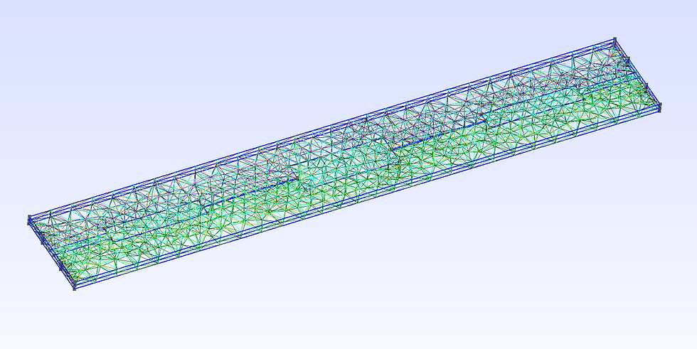
m.generate_mesh()
Next we define our boundary conditions and run the simulation!
port1 = m.mw.bc.ModalPort(p1, 1, TEM=True)
port2 = m.mw.bc.ModalPort(p2, 2, TEM=True)
pec = m.mw.bc.PEC(polies)
sol = m.mw.run_sweep(parallel=True, njobs=4, frequency_groups=8)
The run_sweep function will first compute the boundary modes for the modal port.
We can then post process our results and even use vector fitting to interpolate the results.
gritted_data = sol.scalar.grid
f = np.linspace(0.2e9, 10e9, 2001)
S11 = gritted_data.model_S(1,1,f)
S21 = gritted_data.model_S(2,1,f)
plot_sp(f/1e9, [S11, S21], labels=['S11','S21'], dblim=[-40,6], logx=True)
These results are not 100% accurate. The mesh size is purposefully kept a bit course to make it more manageble for the average computer. Ideally one would refine the conductor boundaries more with these kinds of filters.
We can also plot the real Ez field in 3D
m.display.add_object(pcb, opacity=0.1)
m.display.add_object(polies, opacity=0.5)
m.display.add_surf(*sol.field.find(freq=1e9).cutplane(1*mm, z=-0.75*th*mil).scalar('Ez','real'))
m.display.show()

Comments